|
|
|
|
|
|
|
Dear Professor, dear Scientist, dear Reader,
Over the last 12 months several key new instruments were purchased, enabling once more to extend the portfolio of microscopy techniques and methods available to the researchers of ETH Zurich. Major recent new installations include:
• a plasma Focused Ion Beam Scanning Electron Microscope (FIBSEM) equipped with an ultra-short pulse laser enabling to structure and characterise a broad range of materials from the mm to the nm scale
• a modern multipurpose 200kV Transmission Electron Microscope (TEM) for advanced research in materials science
• two high-throughput screening (light) microscopes
As image data analysis is instrumental to research projects relying on microscopy, we have as well further improved ScopeM IT/software environment and support from experts. Users can now easily get access to
• Windows Virtual Machine (VMs) for processing and analyzing complex multidimensional data
• a performant cryo-EM workflow based on CryoSPARC and ETHZ high-power computing cluster
• support in deep learning for image analysis by our team of experienced image data analysts.
In this Newsletter you will find further information on the above topics, as well as reports on a multi-scale electron microscopy approach developed to study heterogeneous catalysts at work and recent results obtained in the field of super resolution light microscopy.
Finally, I’m pleased to announce that in addition to our numerous other courses (for example our Microscopy Training Program, see link) ScopeM co-organizes again together with EPFL, FMI and the university of Basel the Switzerland Image and Data Analysis School (ZIDAS) - a one-week training program in image analysis for life scientists. Furthermore, ScopeM is hosting the annual FIB workshop under the umbrella of the EUFN network (www.eu-f-n.org/2023-2/).
I wish you enjoy this issue of ScopeM Newsletter, and hope that it will spark further cooperation.
Best regards,
Nicolas Blanc, PhD
Managing Director, ScopeM
|
|
|
|
|
|
|
|
|
|
| Micro-machining and micro-characterization of materials: Possibilities extended by new plasma FIB and laser instrument (Helios 5 Hydra Laser) |
We are very proud to announce the availability of a plasma FIBSEM equipped with laser milling which significantly extends the capabilities of the well-established gallium FIBSEM to larger sample size scales and to a broader range of materials. The “Helios 5 Hydra Laser” combines three beams on one tool focussed in the same coincidence point (Fig. 1). This means that a sample can be imaged by SEM before and after machining by plasma FIB as well as after high-speed milling by the ultra-short pulse laser. Furthermore, elemental analysis by EDS, crystal orientation mapping by EBSD as well as cathodoluminescence imaging are available on this well-equipped beast!
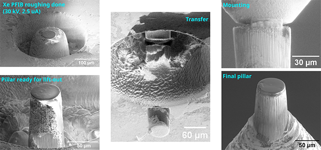
Several projects were already completed by ScopeM experts for various research groups, including for example the preparation of x-ray transparent windows from 3-D printed alumina samples, large lamellae from solid state lithium-ion battery materials and pillars for synchrotron tomography from rock samples. The rock pillars of 60 microns diameter were extracted from specific sites on a chert with microbial fossils (Fig. 2, 3).
Several users, who are in need of established plasma FIB applications like substrate thinning and large cross section milling, have already been trained and are working autonomously on the instrument. We would like to acknowledge the key financial contributions of several research groups that enabled this purchase by adding to the main funds granted by the ETH SEP commission.
Contact: Dr Joakim Reuteler |
 |
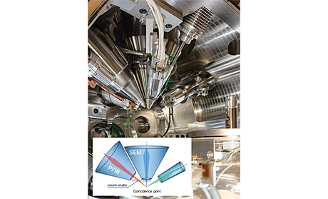 |
| Fig. 1. Photograph looking inside of the sample chamber on the Hydra Laser at ScopeM. Inset: schematic of three-beam setup. (Courtesy of Thermo Fisher Scientific) |
 |
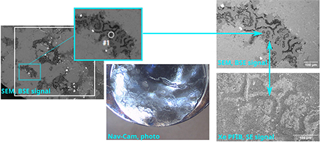 |
| Fig. 2. Localization of target region by means of correlation of SEM BSE image overview map, navigation photograph, SEM BSE and Xe-FIB SE imaging. |
 |
 |
| Fig. 3. Workflow for x-ray tomography pillar |
|
|
|
|
|
|
| New multipurpose JEOL JEM-F200 Transmission Electron Microscope for advanced research in materials science |
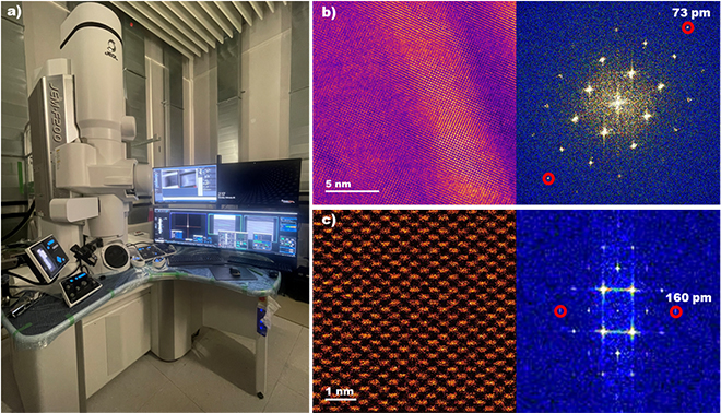
ScopeM is celebrating the successful installation of the multipurpose JEOL JEM-F200 scanning/transmission electron microscope (S/TEM). This advanced microscope can be operated at 80kV or 200kV and be used in various fields of research both in materials science and biology (Fig. 1a). This instrument can be used for the analysis of a broad range of samples such as new metallic alloys, thin films, nanoparticles, single crystals, batteries, ferroelectric and magnetic materials. Its high spatial resolution both in TEM (0.1nm) and in STEM (0.16nm) shown in Fig. 1b and c makes it a powerful tool for investigating the structure and properties of materials at the sub-nanometre scale.
For analytical studies, the system has several key functions enabling accurate and fast phase mapping. It is equipped with an advanced ultra-fast electron energy loss spectrometer (EELS) from GATAN allowing 8000 EELS spectra per second at an energy resolution below 0.5eV due to its bright cold field emission gun. It is also equipped with an energy dispersive X-ray spectroscopy (EDS) system composed of two large silicon drift detectors (each 100 mm2 large), resulting in a total solid angle of 1.7 sr. The system allows fast and precise study of the local chemical and electronic structure at a sub-nanometer. It is also equipped with diffraction imaging (4D-STEM) which maps the local structure or strain in materials at the nanoscale. Electron holography can be performed using a biprism installed inside the microscope enabling direct imaging of magnetic and ferroelectric domains.
The system is also well equipped for in-situ experiments with the availability of heating and cooling holders as well as sample holders dedicated to the study of materials in gas or in liquid environment. Combined with a high-speed 4k x 4k CMOS camera (GATAN Rio 16 camera), in-situ phenomenon can be recorded at a speed of 20fps at full resolution and up to 160fps at 1024 x 1024 pixels.
Overall, the JEM-F200 with its user-friendly interface is a highly advanced and versatile analytical microscope that enables researchers to conduct detailed investigations of materials at the nanoscale, providing a deeper understanding of their structure, composition, and properties. The instrument will be open to users of ScopeM during spring.
Contact: Dr Milivoj Plodinec |
 |
 |
| Figure 1. a) Multipurpose scanning/transmission electron microscope (S/TEM) JEOL JEM-F200 (80 & 200 kV). b) TEM image of [100] Au thin film with the corresponding Fast Fourier Transform (FFT), showing information transfer up to 73 pm. c) High angle annular dark field STEM (HAADF-STEM) image of [110] Si single crystal with corresponding FFT (160 pm). b), c) images are shown in false colours. |
|
|
|
|
|
|
| Two microscopes (Zeiss Celldiscoverer 7) for high-throughput and smart microscopy |
ScopeM recently acquired two automated high-throughput microscopes (Zeiss Celldiscoverer 7) for live cell imaging and smart microscopy or high-throughput imaging. One of them is a wide-field system while the other is also capable of laser scanning confocal and semi super-resolution imaging with the installed LSM-900 and Airyscan 2 options. Both devices are equipped with a plate-loader for extended automated operation and one is even coupled to an automated incubator.
Due to the integrated image analysis module in the Zeiss software (ZEN Blue) and the automated water immersion objective (50x, NA 1.2) they are suited to perform also “smart microscopy”. Smart microscopy describes the connection of automated microscopy and image analysis to generate adaptive imaging workflows. For example, a low-resolution objective and an image analysis pipeline are used to identify regions of interest that can subsequently be imaged in high-resolution.
The devices are compatible with microplates (up to 384 wells) and microscope slides and can be used also for high-throughput screening experiments.
Main contact: Michael Stebler and Joachim Hehl |
|
|
|
|
|
|
| In-Situ Electron Microscopy for Catalysis Studies |
The study of materials in their natural or working state is essential for understanding chemical and physical processes. Such insight is critical to design and optimize materials. Numerous studies have shown that catalysts are metastable and dynamic systems, where the nature of the active state depends on the applied chemical potential and associated chemical dynamic, leading to the formation of transient active sites. Since, the working catalysts are thought to be metastable, the active surfaces could be unstable at non-active conditions, which could lead to the misinterpretation in ex-situ studies of inactive structures as active states.
Moreover, the requirement of high vacuum in electron microscopy has hindered such studies for a very long time. Fortunately, recent progress in the field of in-situ and operando electron microscopy (EM) has allowed real time visualization of working catalysts at high resolution for the first time. In-situ electron microscopy allows to probe the active-state/-sites of catalysts under relevant reaction conditions (temperature, pressure, flow and gas composition) at high spatial and temporal resolution. For instance, due to kinetic and thermodynamic barriers, some catalytic active phases can be formed only at elevated pressures. The reaction pathways, which are irrelevant at low pressure, may become dominant at high pressure and vice-versa. Just simple extrapolation of data obtained at low pressure (10-5 mbar) or high pressures (>1000 mbar) may lead to wrong conclusions. Thus, bridging the pressure and material gaps between fundamental scientific studies of simple model catalyst systems (single crystals, thin foils), which are usually performed at very low pressures and complex industrial catalyst reaction (in so-called “real catalysis”) is of great importance. Therefore, multiscale approach which combine two complementary EM techniques: environmental scanning electron microscopy (ESEM) and in situ gas phase transmission electron microscopy (TEM) is crucial to establish the structure-property relationship across length, time, and complexity scales in catalysis.
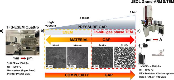
Recently, such approach has been implemented at ScopeM. These cutting-edge techniques: ESEM (pressure: 10-5 Pa-500 Pa; catalysts: thin film, foams, foils), and gas phase TEM (1-1000 mbar, catalysts: metal supported and un-supported nanoparticles) allow to study heterogenous catalysts at work while bridging the pressure and materials gap (Fig 1). It, therefore, provides better understanding of differences and similarities between model and real-world catalysts. In-situ and operando EM studies at ScopeM1-4 over the last 3 years have enabled addressing several scientific questions and projects notably from groups at ETH Zurich working on catalysis. These projects include the study of strong metal-support interaction1-3 , the influence of hydrogen pressure on the structure of platinum−titania catalysts, and the phase coexistence and structural dynamics of redox metal catalysts4.
Contact: Dr Milivoj Plodinec |
 |
 |
Figure 1. Multi-scale electron microscopy approach used to study heterogeneous catalysts at work. a) The Environmental scanning electron microscope (ESEM) TFS Quattro integrated with custom built gas feeding system and Pfeiffer Prisma quadrupole mass spectrometer (QMS). b) A schematic diagram illustrates bridging of pressure and material gap in catalysis. c) The JEOL GRAND-ARM Scanning/transmission electron microscope (S/TEM) combined with DENSsolutions Climate system and HIDEN HAL 3F PIC QMS.
1. Beck, A. et al. Nat Commun 11, 3220 (2020)
2. Beck, A. et al. J. Phys. Chem. C 125, 22531–22538 (2021)
3. Frey, H. et al. Science 376, 982–987 (2022)
4. Huang, X. et al. Adv Mater 33, e2101772 (2021) |
|
|
|
|
|
|
| Fluorescence super-resolution microscopy |
In recent years, fluorescence super-resolution microscopy has revolutionized the way we monitor and visualize /observe biological and molecular processes at the nanoscale. Even though these super-resolution techniques such as STORM, STED and SIM were originally developed and applied in the field of biological sciences, there has also been a range of applications of these methods in the field of physics and materials science.
Single Molecule Localization Microscopy (SMLM) offers the highest spatial resolution, commonly 10-20 nm. This technique is based on the stochastic photo switching of fluorophores, typically controlled via high laser intensity. Nitrogen-Vacancy (NV) centers in diamond are fluorescent crystal defects, where a nitrogen replaces a carbon atom, and one neighboring carbon atom is missing (vacancy). NV centers in diamonds have been praised as stable fluorescence emitters, which do not show any blinking or bleaching. However, NV centers close to the diamond surface (within several nanometers), especially in nanodiamonds show spontaneous blinking which can then be exploited to perform SMLM/STORM imaging.
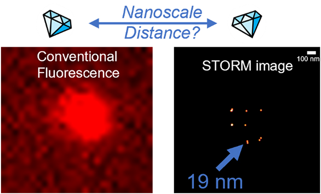
At ScopeM, SMLM /STORM is routinely performed for research projects from various departments using our NSTORM microscope system. In a recent paper, based on research performed at ScopeM with our NSTORM microscope, we were able to localize NV centers in 5 nm nanodiamonds. We also measured distances between two active NV centers in different nanodiamonds down to a precision of ca. 15 nm. For more details check the paper here (DOI: https://doi.org/10.1039/d2na00815g)
|
 |
 |
| Figure 1 summarizes the principle of the experiment. Left: A representative wide-field fluorescence (TIRF) image and right: the corresponding reconstructed super-resolved STORM image of NV centers in 5 nm nanodiamonds under continuous 561 nm excitation: The two images show the same field of view. While in the conventional fluorescence image we cannot discriminate individual spots, the reconstructed image shows several individual localizations of NV centers in nanodiamonds. A distance between two NV centers can be extracted. |
Fluorescent ultra-small nanodiamonds can be potentially used as novel super-resolution labels. This is of biological interest, since the size of the label (ca. 5 nm) becomes comparable to larger proteins. Applications, however, are not restricted to biology. There are alternative optically active defects in diamond (e.g., Silicon-Vacancy defects) or in the so-called 2D materials such as hBN, which could be probed, localized, and characterized using the same setup and SMLM in the future. Such defects in 2D materials are relevant for example in the field of integrated photonics.
For further information on the paper and the method please contact Dr Dorothea Pinotsi.
|
|
|
|
|
|
|
| "Hassle-free" Cryo-EM Data Processing at ScopeM using CryoSPARC |
There has been enormous growth in the field of cryogenic electron microscopy (cryo-EM), since the "resolution-revolution" and the Nobel Prize in 2017. With three Titan Krios microscopes at ScopeM, we typically generate 6 TB of raw data every day.
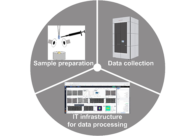
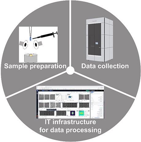
A cryo-EM user faces several challenges that can broadly be categorized as sample preparation, data collection and structure determination (see Figure). ScopeM provides infrastructure, productive training & support tailored to user`s sample for each step. This includes sample preparation & optimization with additive-based kits such as Vitroease [1] or other optimization protocols. We also offer an in-depth one-to-one Titan Krios training for data collection. Since over a year, we have expanded our infrastructure and support to data processing for single particle analysis and helical reconstruction as well. Besides on-the-fly processing during data collection with RELION [2] or cryoSPARC [3], we also provide access to cryoSPARC instances for data processing. |
 |
 |
The message to our user, especially to the new user, is that you don’t have to bother with the purchase/building of Unix workstations or install & maintain relevant software packages. We make it "hassle-free" by providing access to cryoSPARC instances, and together with Central IT and ETH Euler team, take care of maintenance and regular upgrades. A web browser with access to the cryoSPARC instance is all that is required to reconstruct single particle or helical structures from cryo-EM data.
Thus far over 200 projects have been processed on the ScopeM instance and moreover, four additional instances have been deployed for different user groups. Typically, each instance has 100 TB storage, but it can be adapted to user’s requirements. Such infrastructures have received funding support through ETH Zurich’s Scientific Equipment Program as well. Furthermore, to lower the barrier for new users, we offer them adequate storage e.g., 10 TB for about a year for free along with training & support or collaboration to process the data using cryoSPARC.
Some of the advantages of cryoSPARC are: |
| • | | User-friendly and intuitive interface |
| • | | Access via web browser from anywhere |
| • | | Efficient use of computational resources |
| • | | Facilitates real-time collaboration among the users |
| • | | Regularly updated and expanded with new features and capabilities |
|
We encourage users to contact Dr Bilal Quershi for more information and check out following:
[1] http://thermofisher.com/emsampleprep
[2] https://relion.readthedocs.io/en/latest/index.html
[3] https://cryosparc.com/ |
|
|
|
|
|
|
| Virtual Machines for processing and analysis of complex multidimensional microscopic data |
ScopeM has developed, in collaboration with the ETHZ IT-department, several Windows Virtual Machine (VMs) for the processing and analysis of complex multidimensional microscopic data using both licensed and open imaging software. The VMs are directly linked to a « 30 days » central storage of 140 TB dedicated to ScopeM users (scopem-userdata.ethz.ch) located on the same 10Gb/s network area for fast data transfer.
Users of ScopeM microscopes can access the VMs free of charge either via a web-browser client or via the VMware Horizon client. In this way, ScopeM provides a modern IT workplace that better supports location-independent work with up-to-date analyzing software.
To access ScopeM VMs or for more information please contact servicedesk@scopem.ethz.ch. |
|
|
|
|
|
|
| Deep Learning for Image Analysis offered as a service in ScopeM |
| Our team of experienced image data analysts (IDA) is available to assist the community with their image analysis needs through our image clinics' time slots. These remote meetings are held every Monday from 12 to 13 and 13 to 14, and we encourage anyone who requires assistance to join us. We help with data science, deep learning, experimental design as well as training of bioimage analysis tools. Please, book your slot. |
|
|
|
|
|
|
| ZIDAS 2023: training in Image Analysis for Life Scientists |
| The Switzerland Image and Data Analysis School (ZIDAS) offers a focused one-week program that delivers practical, hands-on experience in image processing and analysis, emphasizing biologically relevant applications. As a founding organization, ScopeM strongly encourages its users to apply. ZIDAS is an internationally renowned school, featuring exceptional bioimage instructors from various institutions. Learn more at 2023.zidas.org. |
|
|
|
|